
Details on ZigBee/IEEE802.15.4 Evaluation and Development Kit
This section provides the detailed information on the hardware of the ZigBee / IEEE802.15.4 Evaluation and Development Kit.
- Pin configurations
- Equipped devices
- 2.54mm pitch conversion carrier
- Circuit diagrams
Pin Alignment
CN2 (General-Purpose Connector)

Almost all pins connectable to the wireless engine of the ZigBee/IEEE802.15.4 module are consolidated to CN2 on the sensor node of the ZigBee / IEEE802.15.4 Evaluation and Development Kit. Pin alignment is shown below.
The only difference from J4 of our former kit TWE-EK-001 is Pin 38 (GND for EK-001 and FWP (Flash Write Protect) for EK-002). Connect FWP to either GND or VCC. For details on this pin, see the WP pin of the SPI Flash (or M25P40 for TWE-001 and 001STRONG). If evaluations do not require strictness, this pin can be open.
| Pin No. | Signal | Type | Main Feature | Secondary Feature | Allocation on Board |
|---|---|---|---|---|---|
| 1 | DIO 0 | CMOS | SPI Slave Select 1 (output) | Digital I/O | LCD Chip Select (*) |
| 2 | DIO 1 | CMOS | SPI Slave Select 2 (output) | Digital I/O | LCD CD Signal (*) |
| 3 | DIO 2 | CMOS | SPI Slave Select 3 (output) | Digital I/O | |
| 4 | DIO 3 | CMOS | SPI Slave Select 4 (output) | Digital I/O | |
| 5 | DIO 4 | CMOS | UART0 Clear To Send (input) | Digital I/O | |
| 6 | DIO 5 | CMOS | UART0 Request To Send (input) | Digital I/O | |
| 7 | DIO 6 | CMOS | UART0 Transmit Data (output) | Digital I/O | |
| 8 | DIO 7 | CMOS | UART0 Receive Data (input) | Digital I/O | |
| 9 | DIO 8 | CMOS | Timer0 clock/gate (input) | Digital I/O | LCD RSTn Signal (*) |
| 10 | DIO 9 | CMOS | Timer0 capture (input) | Digital I/O | SW1 Switch 1 |
| 11 | DIO 10 | CMOS | Timer0 PWM (output) | Digital I/O | SW1 Switch 2 |
| 12 | DIO 11 | CMOS | Timer1 clock/gate (input) | Digital I/O | SW3 Switch 3 (*) |
| 13 | DIO 12 | CMOS | Timer1 capture (input) | Digital I/O | Temperature/Humidity Sensor Data |
| 14 | DIO 13 | CMOS | Timer1 PWM (output) | Digital I/O | Temperature/Humidity Sensor Clock |
| 15 | DIO 14 | CMOS | SIF_CLK/IP_CLK | Digital I/O | SMBus Clock |
| 16 | DIO 15 | CMOS | SIF_DATA/IP_DO | Digital I/O | SMBus Data |
| 17 | DIO 16 | CMOS | IP_DI | Digital I/O | LED1 |
| 18 | DIO 17 | CMOS | UART1 Clear To Send (input)/IP_SEL | Digital I/O | LED2 |
| 19 | DIO 18 | CMOS | UART1 Request To Send (input)/IP_INT | Digital I/O | LED3 (*) |
| 20 | DIO 19 | CMOS | UART1 Transmit Data (output) | Digital I/O | LED4 (*) |
| 21 | DIO 20 | CMOS | UART1 Receive Data (input) | Digital I/O | SW4 Switch 4 (*) |
| 22 | SCLK | CMOS | SPI Master Clock Out / Slave Clock In | ||
| 23 | MISO | CMOS | SPI Master In / Slave Out | ||
| 24 | MOSI | CMOS | SPI Master Out / Slave In | ||
| 25 | SSZ | CMOS | SPI Select Out from Jennic IC | ||
| 26 | SSM | CMOS | SPI Select In to FLASH device | ||
| 27 | RESETN | CMOS | Active Low Reset | ||
| 28 | C1P [+] | Analog | Comparator inputs | ||
| 29 | C1M [-] | Analog | Comparator inputs | ||
| 30 | C2P [+] | Analog | Comparator inputs | ||
| 31 | C2M [-] | Analog | Comparator inputs | ||
| 32 | DAC1 | Analog | Digital to Analogue output | ||
| 33 | DAC2 | Analog | Digital to Analogue output | ||
| 34 | ADC1 | Analog | Analogue to Digital input | ||
| 35 | ADC2 | Analog | Analogue to Digital input | ||
| 36 | ADC3 | Analog | Analogue to Digital input | ||
| 37 | ADC4 | Analog | Analogue to Digital input | ||
| 38 | WP | CMOS | Flash Write Protect | ||
| 39 | VCC | VCC | Vcc | ||
| 40 | GND | GND | Ground |
(*) Features available only for the sensor node (large, with the LCD screen)
*The descriptions of signals, main features, or secondary features could vary by data sheets or catalogs. Therefore, you may have to unify them.
J9 and J11 (UART)
The following shows the pin alignment of J9 and J11 on the sensor node of ZigBee / IEEE802.15.4 Evaluation and Development Kit that are connected to UART0 and UART1:
| Pin No. | Signal | Type | Description |
|---|---|---|---|
| 1 | GND | CMOS | Ground |
| 2 | RTS | CMOS | Transmission Request |
| 4 | Rx | CMOS | Received Data |
| 5 | Tx | CMOS | Transmitted Data |
| 6 | CTS | CMOS | Transmittable |


The USB-UART connection cable is connected as shown in the figure on the right. Make sure to insert the cable in the correct direction.
JP4 and JP6 (Jumpers to Select Power Source)
You can select the power source for use by means of a jumper.
Set up the jumpers for JP4 and JP6 on the sensor node of the ZigBee / IEEE802.15.4 Evaluation and Development Kit, according to the procedure below:
AC adapter
Connect the jumper pins to JP4 (1-2) and JP6 (1-2).
Use an AC adapter of 5 to 6 [V] and 0.5A or more.
Use a plug with the internal diameter of 2.1mm, external diameter of 5.5mm, and the positive central polarity. Be aware of the polarity.
USB feed
Connect the jumper pins to JP4 (3-4) and JP6 (1-2).
Connect the USB-UART conversion cable supplied with the Evaluation and Development Kit to UART0 or UART1, and the USB terminal to your computer.
4 x AA batteries
Connect the jumper pins to JP4 (5-6) and JP6 (1-2). (Internal regulator is used)
*In this configuration, do not apply voltage equal to or exceeding 6.4V.
*006P dry cells cannot be used.
*Protect against reverse connection or short-circuit. The fuse (F2) blows in case of emergency to protect the circuit.
2 x AA batteries
Connecting the jumper pins JP4 (5-6) and JP6 (3-4) can directly connect dry cells for use. (Internal regulator is used)
*In this configuration, do not apply voltage equal to or exceeding 3.6V.
*006P dry cells cannot be used.
*Protect against reverse connection or short-circuit. The fuse (F2) blows in case of emergency to protect the circuit.
J6 (LCD Backlight)
The LCD backlight is lit by connecting J6 on the sensor node (with the LCD screen) of the ZigBee / IEEE802.15.4 Evaluation and Development Kit.
JP5 (Current Measurement Pin)
The pins to measure consumption current are mounted.
Pin 1-2 and Pin 3-4 are connected in parallel to the 100mΩ current sensing resistor.
To measure the current of the wireless engine only of the ZigBee/IEEE802.15.4 module, measure the current of Pin 3-4 and divide the value by 100mΩ.
To measure the current of the entire circuit, measure the current of Pin 1-2 and divide the value by 100mΩ. The current consumed by the regulator (IC1) and pilot lamp (D4) is not included.
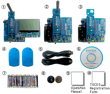
Equipped Devices
LCD
A 128x64 pixel LCD (NHD-C12864A1Z-FSB-GBW-HTT NEWHAVEN DISPLAY) is equipped with the sensor node (with the LCD screen) of the ZigBee / IEEE802.15.4 Evaluation and Development Kit. SPI is used as the interface.
The backlight is turned ON/OFF using the jumper pin (JP1).
*The LCD screen is covered with protection film at the time of shipment. Remove the film as required.
Temperature and Humidity Sensor
The Sensirion high-accuracy sensor SHT-21 is equipped with the sensor node of the ZigBee / IEEE802.15.4 Evaluation and Development Kit. I2C is used as the interface.
Measuring range:
Temperature: -40 to 125
Humidity: 0 to 100%RH
Illuminance Sensor
ROHM BH1715FVC is equipped with the sensor node of the ZigBee / IEEE802.15.4 Evaluation and Development Kit. I2C is used as the interface.
Measuring range:
Equivalent to 0 to 65535 lx
LEDs
LED1 to LED4 (directly driven by DIO)
LED (D1) DIO16
LED (D2) DIO17
LED (D3) DIO18
LED (D4) DIO19
Switches
- SW1 to SW4: Tact switches (Press these switches to change DIO to low)
- SW5: RESETN (Press this switch to reset)
- SW7: Program (Press this switch and reset to move to the program mode)
SW1 DIO9
SW2 DIO10
SW3 DIO11
SW4 DIO20
Fuse (F1)
The 500mA fuse is 0451.500MRL (Digikey) or 0154.500DR of LITTLEFUSE.
2.54mm Pitch Conversion Carrier
The wireless module is connected to the base substrate through the 2.54mm pitch conversion carrier. See 2.54mm Pitch Conversion Carrier for details.
Circuit Diagrams
All circuit diagrams are included in the CD-ROM supplied with ZigBee / IEEE802.15.4 Evaluation and Development Kit to show peripheral circuit designs for your reference.
Wireless Products
- Overview
- Wireless Products Overview
- Wireless Engine
- TWE Lite DIP
- TWE-Lite
- TWE-REGULAR
- TWE-STRONG
- Software
- ToCoNet
- TWE-ZERO
- Evaluation, Development
- Evaluation & Development Kit
- Sensor Network Evaluation Kit
- Antenna
- Avaliable Antennae
Technical Information
- RFID
- 920MHz_vs_24
- IEEE802.15.4
- Protocol Stack
- ZigBee
- Wireless Sensor Networks
- Energy Harvesting Technology
- M2M Wireless Communications
- HEMS / BEMS / FEMS / CEMS
- Internet of Things